Last Update on :
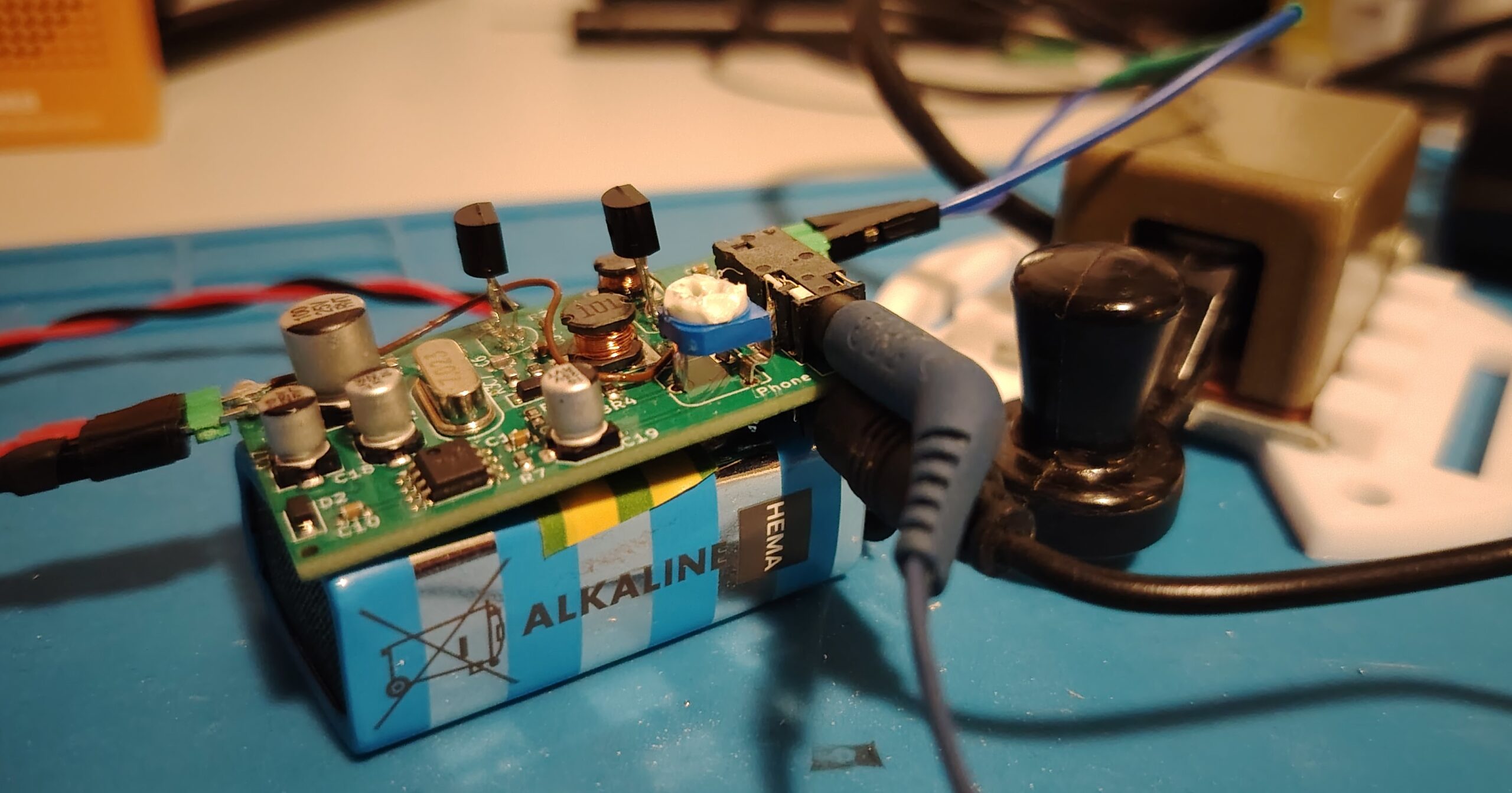
This idea came from a discussion on reddit post talking about K6ARK’s micro pixie operation. As I never tried doing anything in SMD I though it would be a great project to learn the basics. The schematic is really simple, I just took an already working schematic from chinese pixies and reimplemented it in Kicad. Not knowing what size to go for, I chose the size of the recommended power supply for this transceiver when operating in the wild: the 9V battery. Another constraint was that I wanted it to be cheap to manufacture, for the PCB thats easy, going to our favorite low-cost producer JLC PCB. For the SMD assembly, as I don’t have the means to solder those components, I went with JLC PCB assembly, and to make it cheap, SMD components are present only on one side, so reducing the size could be possible by putting SMD components on both faces, or a redesign/rerouting.
The Circuit
The circuit is as described on the schematic on the left. I removed the diode bridge as well as a reverse polarity protection, not my smartest move but I’ll add it back for the next iteration. The buzer was also removed, no place on the PCB as I want it to be compact. Otherwise no modification, for this first version, so we are working with the basic pixie, I’ll check to add a sidetone or improve reception in the next versions. I even used the exact same transistors, athough changing one of the to a 2N2222 could increase the power output of this pixie.

Circuit recovered from: https://w5nor.org/pixie/
PCB mistakes for V0

Quite happy to have only one bodge wire on this PCB ! I misread the circuit and connected the resistor of the display LED to ground instead of Vcc. Correcting this is quite easy, cutting the termal relief to the diode with a diamond tip or scalpel and then the infamous bodge wire is soldered to the LED directly to +9V. The silkscreen of the transistors are reversed, another mistake followed by the two connectors on the side having too small vias to solder the header.
As you can see, I kept some through hole components, mainly transistors, crystals and potentiometer for cost reason as those are premium parts for JLC PCB assembly. The audio LM386, for a reason I can’t figure out, I left as a SMD part, could use through hole to reduce cost further more, as well as the inductors. Will share the corrected version of the PCB and BoM at the end of this post.
Measurement: Power Ouput
Theory
The power output was measurement with oscilloscope measurements on a 50 Ω dummy load, presenting a nice sinusoidal shape during transmission with 13V peak to peak voltage. Using some slight math , we can extract the VRMS value being sure our signal is a sinusoid: $$V_{RMS}=\frac{V_{peak}}{\sqrt{2}}$$ then we can calculate the associated RMS current knowing the resistor is R=50 Ω in our case : $$I_{RMS}=V_{RMS}.R$$ If we then combine the two values we have here in the power equation it gives us: $$P=V.I$$ $$P= \frac{V_{RMS}^{2}}{R} \Rightarrow P=\frac{(\frac{V_{peak}}{\sqrt{2}})^2}{R} $$ We can further simplify the formula to directly use the peak voltage as the in the input: $$ P=\frac{V_{peak}^2}{2.R} $$
Experimental
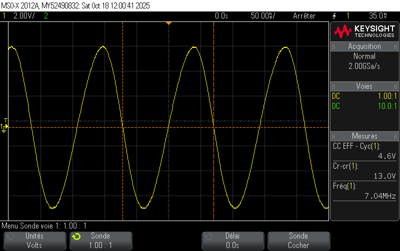
Using this oscilloscope screenshot we have the peak to peak voltage at 13V, we can extract the RMS voltage giving us 4.5926 V, a bit more precise that the value displayed by my oscilloscope. Calculating the power output gives us a total of 422.5 mW of power which is in line with the expected value from other chinese pixies.
Conclusion
This is a first experiment, quite happy with the result and the reduced size. I cannot properly test the receiving side except using two of them and it works dont get me wrong but it will have to wait to have my licence. The transmitting is okay for a pixie, with a correct output so glad it works. Some corrections are made and avalaible in the following section for the gerber and circuit. The next step is a reduction in size and adding some quality of life features. Hope this will go well, and that you find this interesting !
Leave a Reply